 +86 188 1869 1624
 INKBANK01

By INKBANK Technical Editorial Team | 10 November 2026
Last reviewed: 10 November 2026
PCB ink is a functional material used in different stages of printed circuit board manufacturing. The three most important process inks in PCB production are etch resist ink, solder mask ink and legend ink. Each has a different function, cure requirement and failure mode. They are not interchangeable with conductive inks or repair coatings.
The useful question is not simply “Which PCB ink is best?” It is “Which ink has been qualified for this board, this printhead, this cure process and the next production step?”
This guide explains what PCB ink does, where each type enters the production flow and how a well-qualified ink can help reduce production problems.
PCB ink is a specially formulated coating or marking material used in PCB manufacturing. A production ink must remain stable in the printing system, form the required pattern on the board, cure correctly and withstand the downstream processes it is designed to face.
The term “PCB ink” is broad. In this article, it refers to process inks used for:
Etch resist
Solder mask
Legends and component markings
It does not refer to conductive silver, copper or carbon inks used to create electrical conductors, or to hand-applied repair solder mask used outside a controlled production line.
| PCB ink type | What it does | Typical production risk | What the ink must withstand |
|---|---|---|---|
| Etch resist ink | Temporarily protects copper that must remain during etching | Poor resolution, weak adhesion, incomplete stripping or residue | Developer, etchant, stripping chemistry and rinsing |
| Solder mask ink | Forms a permanent insulating and protective layer over selected areas | Mask in pads or vias, uneven coverage, weak adhesion or poor dam formation | Cure, reflow, cleaning, chemical processing and mechanical handling |
| Legend ink | Prints component references, polarity marks, serial numbers and traceability data | Bleeding, low contrast, poor adhesion, yellowing or fading | Cure, reflow, cleaning and handling |
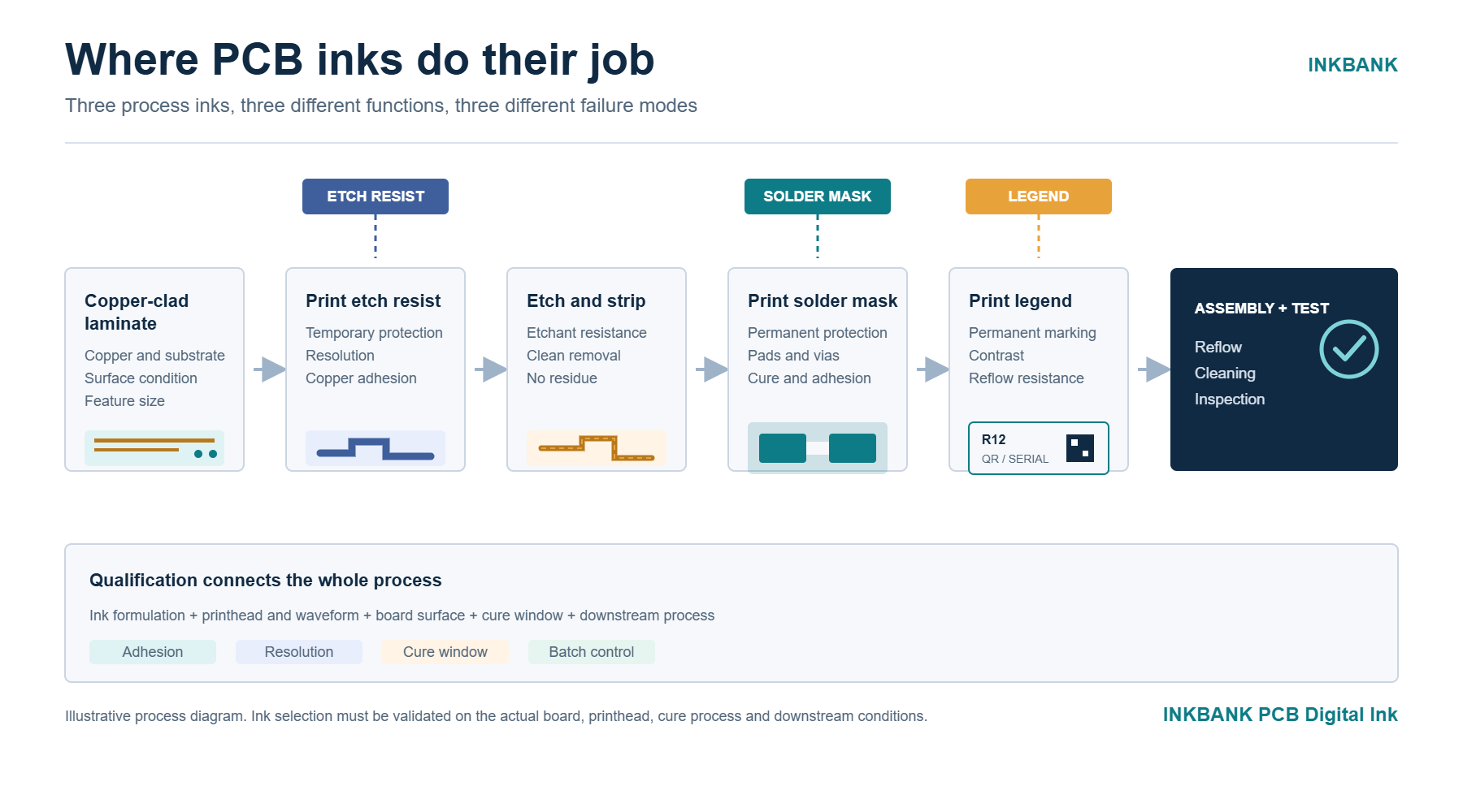
Figure 1. The three process inks perform different functions at different stages of PCB manufacturing. Source: INKBANK process overview, 2026.
Ink is often compared by price per kilogram or per liter. That number is easy to quote, but it does not show whether the material can support a stable process.
A low-cost ink can become expensive if it causes:
Frequent printhead cleaning or replacement
Poor adhesion during reflow or cleaning
Solder mask in pads or vias
Legends that cannot be read after assembly
Etch resist that cannot hold fine features
Repeated sample trials and production delays
Batch-to-batch adjustments
Additional rework, scrap or customer complaints
PCB ink should therefore be evaluated as part of a process window. The ink formulation, printhead, waveform, board surface, cure conditions and downstream process must work together.
Solder mask protects copper traces, helps prevent solder bridging and provides electrical insulation. However, the mask must stay away from areas that require soldering or electrical contact.
Common causes of solder mask in pads or vias include:
Incorrect placement or excessive drop volume
Registration errors
Spreading before cure
Surface-energy differences across copper, laminate and existing resist
Inconsistent cure or insufficient process control
Trace and pad designs that exceed the process window
A production ink with a suitable jetting window and controlled spreading can help place material only where it is needed. The printer, vision system, board handling and cure process remain equally important.
What to verify: printed coverage, mask thickness, dam formation, via clearance, adhesion and cure. Do not approve an ink based on a visual print alone.
Legend information is essential to assembly, testing and maintenance teams. If the markings are faint, blurred or damaged, the board becomes harder to assemble and trace.
Common legend problems include:
Poor adhesion on cured or semi-cured solder mask
Bleeding or feathering on some solder mask colors
Low opacity on dark surfaces
Yellowing after thermal exposure
Cracking, flaking or fading during handling
Clogging after idle time or uneven white pigment dispersion
The correct ink depends on the solder mask color, surface condition, cure method, thermal process and required contrast. White and black legend inks are not automatically interchangeable across every board design.
What to verify: opacity, edge definition, adhesion after cure, adhesion under the actual reflow profile, color stability and printhead recovery after idle time.
Etch resist ink protects the copper that must remain during etching. It must hold the pattern through developer, etchant and rinsing, then release cleanly during stripping.
Typical production problems include:
Loss of fine-line resolution
Poor adhesion on copper
Etchant undercut or pattern defects
Residue after stripping
Incomplete cure or an overly brittle film
Material spreading before cure
Digital etch resist can reduce the need for dry film or photomasks in some production processes. It does not automatically replace every resist process. Board complexity, feature size, throughput and downstream chemistry still determine whether the process fits.
What to verify: minimum feature size, edge quality, adhesion, etch resistance, stripping completeness and residue.
Screen or photomask processes require tooling for each design. When the board, ink and process have been qualified, digital inkjet printing can print directly from a digital file.
This can help production teams that handle:
Prototypes
Small and medium batches
Frequent design changes
High product mix
Short delivery windows
The benefit is not simply “no screen.” The real value is a shorter setup and changeover cycle, less tooling storage and the ability to adjust production without rebuilding a physical image for every design.
Modern PCB production often requires more than the same logo or fixed marking on every board. Serial numbers, QR codes, data matrices and production identifiers can be printed digitally.
This can support:
Unit-level identification
Repair and rework history
Production traceability
Customer or process-specific marking
The limiting factor is not only the ink. Camera calibration, file handling, print resolution, contrast and code verification must also meet the process requirements.
Industrial inkjet printheads have small nozzles and specific fluid requirements. PCB ink must remain compatible with the printhead and ink supply system over time.
Important variables include:
Viscosity and surface tension
Pigment particle size and dispersion stability
Filtration and filter placement
Degassing and bubble control
Recirculation and pressure stability
Sedimentation during storage
Cleaning and recovery after idle time
A well-formulated ink can reduce jetting variation, but it cannot compensate for an unsuitable filter, unstable pressure, trapped air or poor maintenance.
PCB manufacturers cannot re-qualify the process for every drum of ink. They need confidence that key properties remain within an agreed range and that each batch can be traced.
Useful supplier documentation includes:
Technical Data Sheet
Safety Data Sheet
Batch-specific Certificate of Analysis
Storage and shelf-life guidance
Product-specific RoHS and REACH documents
Printhead and cure recommendations
Sample or pilot-test reports
The exact document set depends on the product and the customer's quality management system.
PCB ink should be qualified with the actual board and process, not only with a supplier label.
| Qualification area | What to confirm | Why it matters |
|---|---|---|
| Board and surface | Substrate, copper thickness, solder mask color and state, feature size | The same ink can behave differently on different surfaces |
| Printhead and waveform | Drop size, waveform, maintenance, filtration and ink supply | Jetting performance is a system property |
| Cure window | UV wavelength and dose, thermal profile, film thickness | Appearance does not prove complete cure |
| Adhesion | An approved test method on the actual surface | Prevents peeling and rejects after downstream processes |
| Downstream exposure | Reflow, ENIG, cleaning, chemical treatment, mechanical handling | A failure may appear after printing |
| Performance | Insulation, hardness, chemical resistance or resolution as applicable | Must match the function of the specific ink |
| Batch control | COA, retention samples and incoming inspection | Reduces lot-to-lot variation |
| Production trial | Defined acceptance criteria and sample size | Prevents an unreliable laboratory result from becoming a production promise |
Digital inkjet is often worth evaluating when production includes:
High product mix or frequent changeovers
Short-run or quick-turn orders
Repeated design changes
Variable data or unit-level traceability
A need to reduce screens, films or photomasks
A requirement to deposit material only in selected areas
It may be less attractive when:
The existing screen or photolithography process is already highly optimized for stable long runs
The board design falls well outside the inkjet process window
The production team cannot control cure, filtration, maintenance and ink handling
The required color, appearance or end-use performance has not been demonstrated
The right decision is based on the total process, not on one comparison of print speed or ink price.
Before sampling, ask:
1. Which PCB substrates, solder mask colors and surface conditions have been tested?
2. Which printhead, waveform and ink supply conditions were used?
3. What are the recommended cure and storage conditions?
4. Which test methods support the adhesion, hardness and chemical-resistance claims?
5. Can the supplier provide product-specific TDS, SDS and compliance declarations?
6. What batch controls and COA data are available?
7. What sample information is required: board type, printhead, cure method, feature size and downstream process?
8. What technical support is available if the trial does not meet the acceptance criteria?
INKBANK manufactures PCB legend ink, solder mask ink and etch resist ink within its industrial inkjet ink portfolio. The company has nearly 20 years of ink formulation and manufacturing experience, with laboratory, testing and quality-control resources supporting application development.
INKBANK's PCB product pages currently state REACH and RoHS compliance for the relevant products. Customers should request the latest product-specific declaration and test scope before qualification.
For a useful sample assessment, share:
Board type and copper thickness
Solder mask type and state
Printhead model
Cure method
Feature size and target application
Downstream processes such as reflow, ENIG or cleaning
The current problem or production objective
Request a PCB ink application assessment.
PCB ink is a functional ink used in PCB manufacturing. The main process types are etch resist ink, solder mask ink and legend ink. Each material has a different function and must be qualified against the board, printhead, cure process and downstream manufacturing steps.
No. Conductive ink is designed to form electrical conductors. Etch resist, solder mask and legend inks perform protective, insulating or marking functions. They should not be treated as interchangeable material categories.
The three common process inks are etch resist ink, solder mask ink and legend ink. Conductive carbon, silver or copper inks are separate categories used to form conductive features.
It can result from excess drop volume, registration error, spreading before cure, surface-energy differences or a design outside the process window. The ink supply, printer and cure process must be checked together.
Possible causes include poor adhesion to the solder mask, incomplete cure, thermal exposure, incompatible surface chemistry or batch variation. The actual reflow profile and board surface should be included in the test.
It can replace some screen-printing steps when the board, volume, feature size and process are suitable. It is not a universal replacement. High-volume stable production and some special applications may still be better served by another process.
A useful TDS should describe the product, recommended use, typical physical properties, cure conditions, storage, handling, performance data and test methods. Product-specific compliance and batch documents should be requested separately.
Test with the actual substrate and downstream process. Record the printhead, waveform, cure profile, film thickness and test method. Evaluate appearance, adhesion, resolution or insulation as applicable, then define batch and production acceptance criteria.
PCB digital inkjet overview
PCB white and black legend ink
PCB solder mask ink
PCB etch resist ink
Contact Us
Hello, welcome to submit any questions and suggestions. We will reply to you as soon as possible. Thank you for your support and help.


